
3D technique enhances bio-inspired hierarchical structures
A team of researchers from Changchun University of Science and Technology, China, have developed a novel method for the rapid and maskless fabrication of bio-inspired hierarchical structures, using a technique called laser interference lithography. Specifically, the researchers use the interference pattern of three-and four-beam lasers to fabricate ordered multi-scale surface structures on silicon substrates, with the pattern of hierarchical structures controllable by adjusting the parameters of incident light.
In accordance with the theoretical and computer analysis, the researchers have experimentally demonstrated the novel technique's potential in large-area, low-cost and high-volume 3D fabrication of micro and nanostructures. This week in the journal Applied Optics, from The Optical Society (OSA), the researchers describe the work.
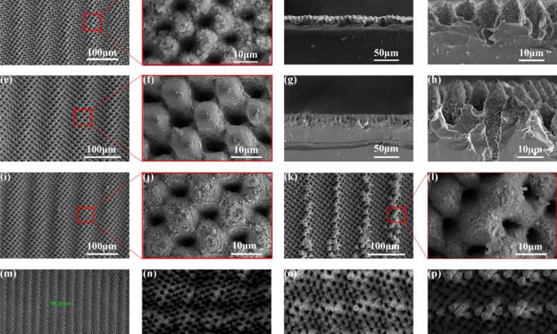
Hierarchical anisotropy and isotropy surface structures can be fabricated by this method with the control of the parameters of each incident beam, which is in accordance with the theoretical analysis and computer simulations. Credit: Zuobin Wang/Changchun University of Science and Technology, China
"We presented a flexible and direct method for fabricating ordered multi-scale 3D structures using three- and four-beam interference lithography," said Zuobin Wang, the primary author and a professor of International Research Centre for Nano Handling and Manufacturing of China at the Changchun University of Science and Technology, China. "Compared with other patterning technologies, our method is simple and efficient in terms of obtaining bio-inspired hierarchical structures."
Wang mentioned that for certain complicated surface structures, conventional techniques such as electron beam lithography may take several hours or a day to fabricate the pattern, while the laser interference approach only takes several minutes to generate the structure, which makes the technique suitable for high-volume industrial production.
"Laser interference lithography is a maskless patterning technique that uses the interference patterns generated from two or several coherent laser beams to fabricate micro and nanometer periodic patterns over large areas," Wang said.
Different from conventional patterning techniques like electron beam lithography, the laser interference technique enables fabricating the entire substrate surface with one single exposure or one-step lithography.
For example, in Wang's experiment, the one-dimension multi-scale structure, that is, one-dimension oriented arrangement with the sinusoidal grooves covered with periodic line-like structures was fabricated by exposing the silicon substrate to three or four interfered beams for one time.
The resultant surface pattern, though arranged in one direction, has three-dimension spatial structure. To obtain more complicated structures such as two-dimension oriented multi-scale structures, the researchers simply rotated the substrate by 90 degrees in the plane and applied second laser exposure to the surface.
According to Wang, their experimental process is simple: a high power laser beam was split into three or four equal beams, which then were directed by mirrors to generate interference patterns to fabricate the surface structures.
The laser parameters such as incident angle and azimuthal angle of each beam were adjusted by beam splitters and mirror positions. Other optical devices such as quarter-wave plates and polarizers were used to select the polarization mode and control the energy of laser beams.
According to Wang, the proposed technique could be used to fabricate optical or medical devices such as solar cells, antireflective coatings, self-cleaning and antibacterial surfaces and long-life artificial hip joints.
The researchers' next step is to develop functional surface structures with controllable wettability, adhesion and reflectivity properties for optical, medical and mechanical applications.
Product Spotlight
APV1111GVY
Panasonic

Panasonic PhotoMOS® Photovoltaic MOSFET High-Power Drivers
| SKU: | |
|---|---|
| Stock: | 3490 |
| Cost: | $3.95 |
