
Copper etch scheme overcomes resistivity & reliability issues
At the recent IEEE IITC conference in Grenoble, France, nanoelectronics research center imec and Tokyo Electron Limited jointly presented a direct copper etch scheme for patterning Cu interconnects. The scheme has great potential to overcome resistivity and reliability issues that occur while scaling conventional Cu damascene interconnects for advanced nodes.
Aggressive scaling of damascene Cu interconnects leads to a drastic increase in the resistivity of the Cu wires, due to the fact that grain size is limited by the damascene trenches, which results in increased grain boundary and surface scattering. Additionally, the grain boundary negatively influences electromigration. When scaling damascene Cu interconnects, reliability issues occur because the overall copper volume is reduced and interfaces become dominant.
Imec and TEL have demonstrated the feasibility of a direct Cu etch scheme to replace the conventional Cu damascene process. A key advantage of the direct Cu etch process is that it systematically results in larger grain sizes. Electromigration performance is preserved by applying an in-situ SiN cap layer that protects the Cu wires from oxidation and serves as the Cu interface.
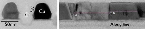
TEM section of copper etched lines encapsulated by SiN cap layer
The results were achieved in co-operation with imec’s key partners in its core CMOS programs GLOBALFOUNDRIES, Intel, Micron Technology, Panasonic, Samsung Electronics, Taiwan Semiconductor Manufacturing, SK Hynix, Fujitsu Semiconductor, and Sony.
Product Spotlight
APV1111GVY
Panasonic

Panasonic PhotoMOS® Photovoltaic MOSFET High-Power Drivers
| SKU: | |
|---|---|
| Stock: | 3490 |
| Cost: | $3.95 |
