
Could graphene FETs drive greater RF integration?
There is growing anticipation that graphene will soon emerge as a replacement for silicon, fuelled by its outstanding promise. Now, a lack of progress towards monolithic integration may have turned an important corner thanks to the latest R&D breakthroughs, as Philip Ling reports.
Graphene FETs (GFETs) have been shown to deliver intrinsic benefits in RF applications, such as unity current gain frequencies higher than 400GHz and (theoretical) operating frequencies exceeding 500GHz. But despite a significant amount of effort having been applied to developing and improving many aspects of GFETs, such as the graphene materials, gate dielectrics and device architectures, their use in RF applications hasn’t followed.
Most of the results available today relate to discrete transistors and externally connected passive components, and while these examples show promise if the technology is to be fully commercialised a truly monolithic solution is required. Of the few monolithic demonstrations made, the conventional process flow of first constructing the active device and then applying a series of back-end-of-line (BEOL) processes to complete the IC have been shown to cause deterioration in the GFET, due to the delicacy of the graphene.
Recently, however, researchers at IBM presented results of a multi-stage graphene RF IC fabricated in a standard silicon fab. In order to overcome the problem of device degradations, the researchers decided to completely reverse the fabrication flow; by building all the passive components together with device gates on an 8" silicon wafer before the graphene films are applied. Furthermore, the team says the same process can be applied to any channel materials that can be transferred, such as carbon nanotubes or other two-dimensional nano materials.
Standard flow, backwards
The process can be implemented using a standard silicon BEOL flow; four metal layers were required for the demonstration chip which illustrates how the passive-first, active-last flow first sees inductors and the bottom plate of capacitors being formed on metal layer 1, followed by metal layer 2 becoming both the top plate of the capacitors and the bottom part of the T-shaped gate. Metal layer 3 forms the top of the gate, which is then followed by the dielectric formed using atomic layer deposition. Chemical vapour deposition was then used for the graphene transfer. Resistors and drain/source contacts were formed using metal layer 4.
The researchers reported that the T-shaped gate structure and multiple-finger design delivered very low gate resistance while maintaining short channel length, leading to notably improved maximum operating frequency.
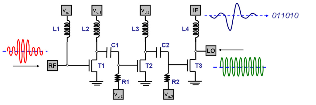
Figure 1: The circuit designed was a three-stage RF front-end
The IC constructed comprises eleven components, as shown in Figure 1. The circuit designed is an RF front-end with three stages; each stage is connected to the next through capacitive coupling, allowing the gate bias voltage of each stage to be individually adjusted. The first two stages are band-pass amplifiers to provide both amplification and filtering. The third stage performs mixing with a local oscillator (LO) signal, to down-convert the GHz RF signal to an intermediate frequency in the MHz range.
A key feature of this process flow is fabricating the GFET at the last step, as it prevents it from being damaged in the harsh BEOL processes, such as chemical mechanical polishing and Cu electroplating. This could be seen in the transfer characteristics and peak transconductance. In addition, low output conductance shows clear drain current saturation, which delivers high intrinsic gain.
Performance
Before testing the IC as an RF receiver it was used to drive a 50Ohm load, where it demonstrated a power gain of +4dB; the first graphene IC able to perform amplification when loaded with 50Ohm impedance. Also, stability was shown to be excellent, with less than +/-1dB variation over a testing period of more than 20 hours.
When tested as a receiver the circuit out-performed previously demonstrated circuits; with 50 times higher conversion gain with 200 times smaller LO power. A low power LO prevents it from impacting the IF output. Furthermore the three-stage IC consumed less than 20mW, which is 600% less than a single-stage graphene IC previously referenced.
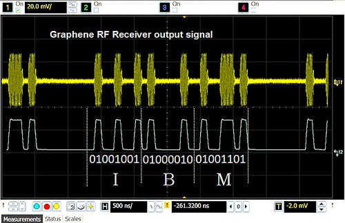
Figure 2: The ASCII code for 'IBM' was successfully received and demodulated
To demonstrate the functionality, an RF carrier of 4.3GHz was amplitude modulated with a 16-bit stream and applied to the receiver, to mimic the typical digital data transmitted using a wireless carrier. The results indicate a high quality receiver function had been achieved, by allowing the original binary code to be recovered by rectification and low-pass filtering. Figure 2 shows how the ASCII code for IBM was successfully received and demodulated.
The team believes that the IC demonstrated multifunctional RF circuits are feasible using the grapheme-last flow using a silicon fab, leading to heterogenous 3D system integration with a silicon CMOS backbone. This could result in high performance graphene RF circuits being built directly on top of high-density CMOS logic, to create extremely low-cost, ultra-compact communication systems.
Product Spotlight
APV1111GVY
Panasonic

Panasonic PhotoMOS® Photovoltaic MOSFET High-Power Drivers
| SKU: | |
|---|---|
| Stock: | 3490 |
| Cost: | $3.95 |
